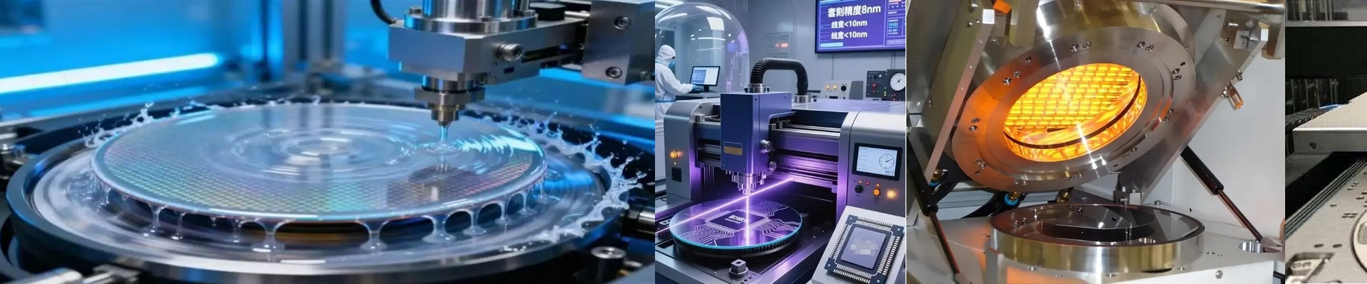
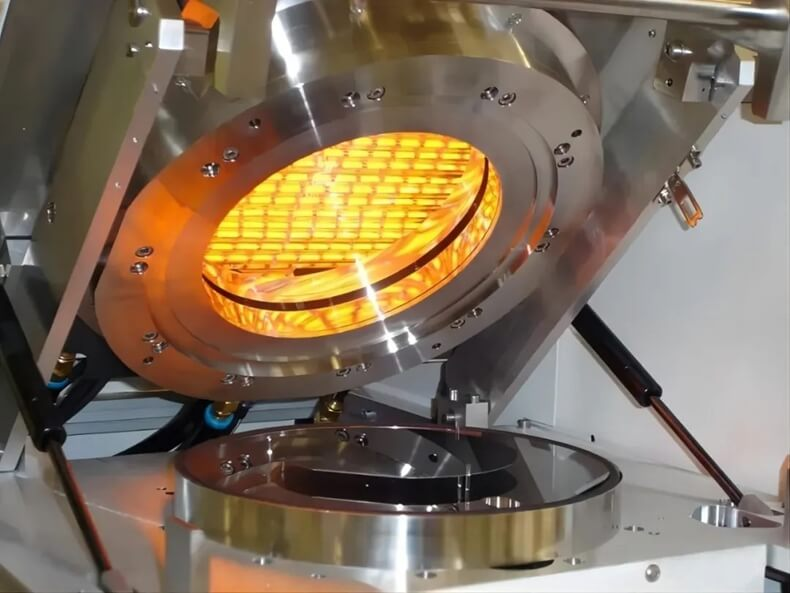
On the line, wafer drying isn’t a passive box to check—it’s the last thermal gate before pattern integrity locks in. Leave behind even a little moisture, or let the bake profile drift during soft bake or hard bake, and you’re inviting photoresist skinning, edge bead, and dimensional drift. The solar cell wafer drying lamp was built to take that variability off the table. What matters under the hood We lean on NIR emitters for fast, direct energy transfer straight into the wafer. That cuts thermal lag and keeps the process window stable. The system holds wafer-level uniformity within ±0.1°C across the active area, so the critical bake profiles stay repeatable, lot after lot. Cleanroom compatibility isn’t an afterthought—Class 1–100 environments see no particle spike from the lamp head, and the quartz/reflector assembly is set up to avoid any outgassing that could contaminate photoresist. Output stays steady over 5,000+ hours with less than 5% intensity drift, which means fewer requalifications and less unplanned downtime. Why it fits in solar wafer fabs In solar fabs running lithography, the lamp drops right into the drying/bake sequence without reworking the track recipe. Tighter thermal control shortens settling time, trims scrap and rework, and keeps the line moving. NIR efficiency and precise dwell control cut energy use, and the long emitter life eases the spares burden and stretches maintenance windows. The upshot is process stability you can audit: photoresist behaves consistently, critical dimensions stay predictable, and yield excursions tied to drying drop off. Here’s the catch: NIR drying is line-of-sight, so wafer geometry and carrier shadowing have to be baked into the fixture design. Profile matching takes a short qualification run to dial in power, dwell, and beam angle for your exact thickness and anti-reflective coating stack. Once calibrated, the system runs with minimal tuning—but that upfront setup is what earns you the ±0.1°C uniformity in production.