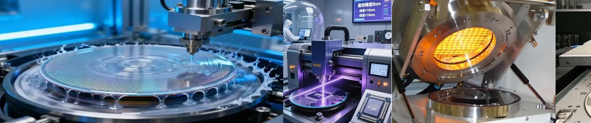
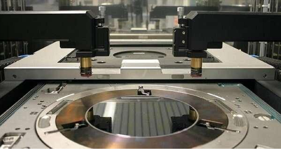
Out on the line, wafer thinning is a thermally sensitive operation. Thin silicon cracks when the thermal budget isn’t handled cleanly, and a 2°C swing across the surface can set up stress non-uniformity that shows up later as yield loss. We built our infrared heating platform around that constraint: controlled, fast, and repeatable heat delivery where the wafer has zero margin. What matters is the physics and the control. The system hits near-infrared wavelengths that line up with strong silicon absorption bands, so energy dumps in quickly with minimal substrate heating. Temperature is measured in-situ and held to ±0.1°C across the chuck, which translates directly into tighter process windows for the soft bake and hard bake steps that sit next to thinning. Cleanroom fit isn’t an afterthought, either — the assembly is built for Class 1–100, with materials and seals that keep particle generation near zero and make routine ISO Class 5 validation straightforward. Here’s why it works in practice. Thinning needs heat that ramps fast, but it has to be even. The infrared module delivers that rapid ramp-up without hot spots, improving thickness consistency and cutting scrap from micro-cracks. The payoff shows up as fewer rework lots, stable uptime, and thermal profiles you can count on lot after lot. Energy use drops too, because the source is efficient and the dwell time is shorter. One practical heads-up: the module is compact, but it needs a dedicated clean power feed and verified emissivity data for your wafer stack. Plan a short qualification run to lock the recipe, and confirm your existing thinning tool can take the closed-loop thermal signals. Once the interface is aligned, the process runs with the kind of stability semiconductor manufacturing demands.